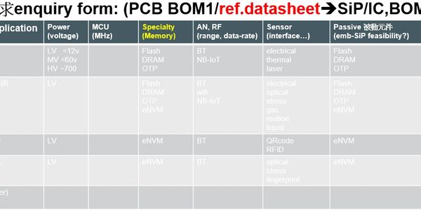
facilitate system/BOM1=> BOM2 migration:
[as-is] status quote

from 0(idea) to 1(proof-of-concept, EVB)
[to-be] design-for-resilience strategy

1(reference BOM) ->2(NRE$, revision) ->N(production)

design-for-system application (I)
其他資訊
- likely reuse the sub-system architecture (module);
- leverage chips in the markets, and create own differentiated chiplets/interface;
- strategy for design-for-supply chains;
- decent PDC (product development cycle) and time-to-markets revision.
[chiplets/package path-finding]:
cloud-mode thermal assessment:
https://fusion-sip-chipthermaldesign-en.pages.dev/chip_design
DfX: DfM examples


DfX: MfD examples


design-for-decent IP/chiplets/adv-SiP

partition/blocks vs. chiplets interconnection

DCD IPs for automotive interface, safety & security

design-for-supplychain resilience
其他資訊
4. matching IP vs. technology (process, sip, designs);
5. re-usability among applications: industry, automotive, space, etc.
6. practical design for supplychain options & operations.
=> talk to the experienced expertise.

ex11: MEMS+CMOS/SiP accelerator
其他資訊
(it-was) >5 years for MEMS 0->1 PDC efforts;
(to-be) <1.5 years with proven-MEMS IP+process (minor tuning),
we help to improve 1->2/N PDC in <2 years, by decent/flexible
"AinterposerX" methodologies.
ex12: physical edge-AI prototyping


ex31: MEM-stack/SiP accelerator
其他資訊
(it-was) MEM-KGD for dram/flash/sram assembly as PCB/PoP;
(to-be) MEM-hybrid for D2W, W2W interposer integration.
訂閱
註冊即可搶先得知最新資訊。